Optoeletronic investigation of Cu2ZnSn(S,Se)4 thin-films & Cu2ZnSn(S,Se)4/CdS interface with scanning probe microscopy
Jiangjun Li, Yugang Zou, Ting Chen, Jinsong Hu, Dong Wang , Li-Jun Wan
Sci. China Chem., 2016, 59, 231-236
Abstract (click for pdf file)
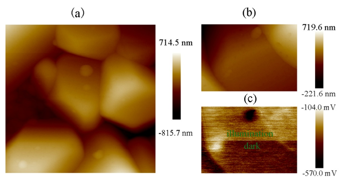
The kesterite-structured semiconductor Cu2ZnSn(S,Se)4 (CZTSSe) is prepared by spin coating a non-hydrazine precursor and annealing at Se atmosphere. Local electrical and optoelectronic properties of the CZTSSe thin-film are explored by Kelvin probe force microscopy and conductive atomic force microscopy. Before and after irradiation, no marked potential bending and very low current flow are observed at GBs, suggesting that GBs behave as a charge recombination site and an obstacle for charge transport. Furthermore, CdS nano-islands are synthesized via successive ionic layer adsorption and reaction (SILAR) method on the surface of CZTSSe. By comparing the work function and current flow change of CZTSSe and CdS in dark and under illumination, we demonstrate photo-induced electrons and holes are separated at the interface of p-n junction and transferred in CdS and CZTSSe, respectively.